Foundation Of VLSI Design L1

Other Details

Duration

Btech | Mtech Prer-final Year

  • 12-14months

Btech | Mtech Final Year

  • 6-9months

Passout Candidates

  • 6-9months

Mode of Delivery

Offline - Noida

Note:

  • Because of Pandemic - We are operating in both mode right now (Offline & Online)

Trainers

Mr. Puneet Mittal

  • He is Founder and CEO of VLSI Expert Pvt. Ltd. He is very much passionate about the teaching and mentoring to students. He has 14+ Semiconductor Industry experience. Know more about him

Other Industry Trainers

  • Trainers from our associated company Like Technoready
  • Industry Experts from Cadence & Synopsys as a Guest Invite
  • Average Experience of 10+years in Semiconductor Industry

Fee Structure

Rs 55,000/- Only

Note:-

  • Inclusive all Taxes
  • Please don't ask for any discount. It's already at minimum price
  • Payment can be done in 2 Instalments (60% & 40% ratio)
  • Payment link can be share on request basis

Contact us

support@vlsiexpert.com

Upcoming batch

Check our calender section

Foundation Of VLSI Design L1

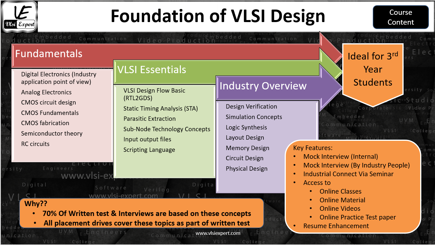
This course is specially designed for the Freshers. As name says it's a foundation course. Every Company first focuses on the fundamental of the engineering subjects.WRITE SHORT SUMMARY.

About the course

Highlight Of Course

Btech | Mtech Prer-final Year

  • 12-14months

Key Features

Offline - Noida

Associated Profiles in VLSI Industry

Why Should I join?

What will I achieve from this?

Contact Us

support@vlsiexpert.com

Upcoming batch

Check our calender section

Student's Review

Madhuparna Das

We can't predict our future. But we can make choices & wish that things placed in the right place. One of my students Madhuparna Das also dreamed similar thing long back and we (#VLSI Expert Family member) all feel proud that she is now in Cadence Design Systems. Like I always say- "Be Expert By Expert"

College: Accurate Institute of Management and Technology - Greater Noida
Year of Passing: 2018
Placement/year: Cadence /2018 (as Intern)
Current Status: In Cadence (Permanent)
Profile: STA Engineer

Geetika Singh

Understanding about #VLSI Industry & it's requirement before Training Vs after Training. One of my #student "Geetika Singh" placed in "Synopsys Inc" after successfully clearing 4-5 rounds. It's her #dream #company & I am happy that she cracked that. Her passion, efforts, hard-work & believe in herself are the only few reasons for her success.
#Fundamentals & #Basics are the foundation of every Industry but unfortunately, students are lacking big time in this area. As a VlsiExpert offline Training Program, I am focusing on this aspect. EDA tools can change, tool's command can change but tool's fundamental can't be changed. We are Engineers - "Tools should not command us - we should command Tools."
You should listen to this 2.5min Video & I can bet it will #motivate every fresher.

College: ABES Engineering College
Year of Passing: 2018
Placement/year: Synopsys /2018 (as Intern)
Current Status: In Synopsys (Permanent)
Profile: Standard Cell Layout Design

Other Video review ...

Rishu Shukla

https://www.linkedin.com/in/rishu-shukla-227631126/

College: ABES Engineer College
Year of Passing: 2018
Placement/year: Synopsys-Gatelength / 2019
Current Status: In Synopsys (Contractor)
Profile: Memory Layout Profile

When I look back on my journey of achieving what I want to be, I see the guidance, motivation and great support of my mentor Puneet Mittal sir which has led me finally to get into a VLSI industry. And a special thanks to Avnish Shukla sir for their help and support.When I was persuing b.tech I did not have an iota about VLSI and I never thought of getting into the core industry. Even when I get to know about VLSI then also I had doubts whether I will be able to achieve this or not. But one person who had a trust and belief on my capabilities was Puneet sir.
In VLSI EXPERT you don't just mug up the concepts and get a placement. You grow over here. Your personality, self belief, way of learning, attitude is developed over here. Just follow the instructions of Puneet sir and you will see a vast change in your learning and in all the other aspects.
In my case I had a doubt whether I will be able to achieve this or not one year back but he took out the best of me.He motivated me everytime whenever I felt low. Sir you are the reason I didn't give up. This journey is never be possible without you. Thank you for all your love and support.

Shriya Jain

https://www.linkedin.com/in/shriya-jain-503514145/

College: JP Engineering College - Noida
Year of Passing: 2019
Placement/year: Cadence / 2019 (As Intern)
Current Status: In Cadence (Intern)
Profile: STA Profile (Timing Team)

You have been a great mentor, teacher or guide.Thank you, sir, for encouraging me during my difficult times.I will always be grateful for the knowledge & skills that I gained from you.Thank you once again, sir
#God of STA

Shraddha Maheshwari

https://www.linkedin.com/in/shraddha-maheshwari-5365b3128/

College: ABES Engineering College
Year of Passing: 2019
Placement/year: Synopsys / 2019 (As Intern)
Current Status: In Synopsys (Intern)
Profile: Physical Design Engineer

Your continous support and faith in the person turns eveything possible. I have learnt a lot from you and your discussions with us. You don't only help us in developing skills but also shape our attitude towards learning and life. I don't understand how you manage your time to be available for us whenever we are in some trouble. It was all your belief in me and our conversations. The time when you said "mujh par vishwas hai ya nahi" was the point for my motivation. You even provided me a platform (as junior lab assisstant) to share what i have learnt with my mates which helped me to overcome my shortcomings. Thanks a lot sir for your motivation, time and constant support. Your mantra "you just need one opportunity" and "you are not going to lose anything but seekhne ko bht hai" will remain my motivation.
-Thank you sir 😇

Other writen review ...

What Industry Experts Says about this course


Course Content

  • Module 1: Digital Electronics
  • Module 2: Semiconductor Electronics
  • Module 3: CMOS Design
  • Module 4: CMOS Design in VLSI Design
  • Module 5: Standard Cell Layout Design
  • Module 6: VLSI Automation Concepts and QOR
  • Module 7: Logic Synthesis
  • Module 8: Static Timing Analysis
  • Module 9: Memory Circuit Design
  • Module 10: DFT Concepts
  • Module 11: Low Power Methodology
  • Module 12: ASIC Flow and Physical Design
  • Module 13: Verilog
  • MODULE 14: ADD-ONS

Module 1: Digital Electronics

Digital basics (Revision of Engineering course work)

  • Binary System, Logic Levels, Different Logic States, Noise Margins
  • Combinational circuit & Sequential circuit,Frequency Divider/Multiplyer Circuit,Sequence Detector
  • FSM (Meely and Moree Models)

Advance Digital (Implementation of Digital circuit in VLSI design)

  • Designing of Different Logic gates/Combinational Circuit/Sequential elements using MUX
  • PAL, PLA concepts, Tristate Buffers / Tristate Inverter,Clock Gating Concepts
  • Standard Cell Library Concepts
  • Logic Optimization

Module 2: Semiconductor Electronics

Semiconductor Overview

  • Property & Parameter : (Doping/Impurities,Amount of Impurities, Different type of Region (N+/N++, P+/P++),Energy Bands, Fermi Level,Drift Current, Mobility)
  • Semiconductor Devices : (Depletion region, Build In potential,Immobile Ions,Diffusion Current, Recombination)

Module 3: CMOS Design

CMOS Fundamental

  • Basic : (Concepts of Vt in a MOS & Subthreshold Regions, MOS Electrical Parameters: Inout output characteristics,How Source/Drain Terminals are defined,Cross Section of NMOS,PMOS,CMOS,Finfet Vs Planner CMOS)
  • Advance CMOS : ("Different factors on which Vt has dependency, Body Biasing, Channel Length Modulation", FInFet Concepts, W/L Ration Concepts (Parallel and Series Connection),Parameter Varaition (Fast and Slow Transistor) FF/SS CMOS, HVT / LVT / RVT Cells,Device Scalling)

CMOS Circuit Design

  • CMOS Pass Transistor : (Switching Theory,NMOS and PMOS pass Transistor, Transmission Gate concepts, Pass transistor based problems)
  • CMOS Circuit Design : (Designing of all Logic Gates, Combinational & Sequential Circuit)

CMOS Fabrication

  • Cross Section of CMOS,Single Tub/ Twin Tub, Single Well
  • Device Cap and Metal Cap / CMOS Fabrication Process (Step by Step)
  • Shallow Trench Isolation (STI layer), Latch Up Concepts

Module 4: CMOS Design in VLSI Design

Advance CMOS Design

  • CMOS Design : (Temperature Variation, Supply Voltage Variation, Process Variation,PVT Corners,Tap Cells, 3 Terminal & 4 Terminal Devices)
  • Power Dissipations (Static , Dynamic Power, Transition Current, Short Circuit Power Dissipations, CMOS Leakages: Leakage related short circuit current, static current)

Schematic & Simulation Concepts (Include Practical Labs)

  • Schematic of Different Logic Gates : (BSIM Models, SPICE Netlist, Model Files)
  • Fan-In, Fan-out, Driving Strength
  • Introduction to Virtuoso/Tanner & different settings
  • Technology File and different Inputs files

Module 5: Standard Cell Layout Design

Layout Design (Theoritical Concepts)

  • Different layers Understanding, Metal Stack Concepts, Different DRC Rules & their understanding
  • Layout drawing using Paper and Pen
  • Fingering concepts
  • TapCells , Nwell Cells Layout Concepts, Well Proximity Effect (WPE)
  • Latchup and it's preventions, Introduction of Guard Ring
  • Placement of Standard cell in Design(Concepts of SiteRows/Grids/Tracks/Flipping of Standard Cells)
  • Antenna Effects (Concepts, Damage, Remedies),Jumpers, Antenna Diode, Electromigration concepts and it's preventions, AC/DC EM, IR Analysis, Power planning methods to reduce IR, Shielding Concepts

Layout Design (Practical Tool based)

  • Introduction to Virtuoso Layout window & different settings, Layout Pallets, GUI Interface
  • Concepts of DRC, LVS, ERC and Basic Checks (Soft Check)
  • Metal Stack based Design (Like Use both M1, M2 for design)

Module 6: VLSI Automation Concepts and QOR

Unix

  • Overview of Unix platform & Different commands
  • Shell Scripting: bash cshell,awk,sed
  • VI editor concepts

TCL & Perl Scripting

  • TCL & Perl Introduction and it's industrial use,Concepts of Wrapper,
  • Procedure in TCL & regular expression
  • File Handling, Read/Write Operation, Flow Control (Foreach, while, switches, for etc)
  • Perl: List, Hash concepts

QOR and Reporting Concepts

  • Reporting concepts & different analysis concepts
  • Log file and different type of Messages in that ( ERROR Messages, INFO Messages, WARNING Messages)
  • Regression Concepts,Version to Version Check , Accuracy Check, Golden Vs Test Result
  • Automation For Validation
  • How to create charts, read charts, Histrogram, Pi charts concepts

Module 7: Logic Synthesis

Logic Synthesis (basic)

  • Introduction to Synthesis, Basic Terminology
  • Netlist Overview with libraries introduction (Target Library, Link Library)
  • Concept of Synthesizable RTL, Mapping to Gatelevel Netlist
  • Different way of Modelling combinational or sequential elements

Logic Synthesis (Advance)

  • Timing constriant basic (Max Trans, Max Cap, Max Fanout, Min cap)
  • Commonly Faced Issues during Synthesis
  • CDC and LINT Concepts
  • DFT insertion basics inside synthesis tool

Module 8: Static Timing Analysis

Introduction to Static Timing Analysis & Timing Arc

  • Importance of Timing Analysis, VLSI Flow Introduction & different stages where Timing analysis happen
  • Different component of Timing analysis (Timing Budgeting,Timing Constraint,Timing Check,Timing Violations,Fixing of Timing Violations
  • Introduction about different input and output files for STA
  • Importance of Timing Arc & Timing Arc Representation in .LIB Files

Delay Introduction (Cell Delay and Net Delay)

  • Introduction of Delay Concepts
  • Combinational Path Delays,Sequential Path Delays
  • Net Delay basic (Metal Wire Concepts,Metal Stack concepts)
  • Gate Delay Concepts (Charging & Discharging concepts, Load related Concepts, Delay dependency on current of Inverter,Internal Capacitance,Input Capacitance and Output Capacitance concepts

Delay Models & Understanding Delays Libraries

  • Gate Delay Models (How delay depends on Input Transition & Output Load,NLDM Library & CCS Library)
  • Net Delay Models (Transmission Line Models,Elmore Model,Wire Load Model

STA Tool Delay Calculation Methodology

  • Delay Calculation by STA tools (Path based Analysis and Graph Based Analysis)
  • Pre-Layout Delay (using wire-load model) & Post layout Delay (using SPEF File) calculation
  • Delay Calculation using Delay tables, Complexity across different corners.
  • Dependency of Delay on different parameters (PVT Corners,Manufacturing defects,RC Corners)

Timing Paths, Timing Exceptions & Timing Constraints

  • Various Timing Paths (Data Path, Clock Path, Asynchronous Path,Clock Group Introduction
  • Representation of Timing path within Timing report
  • Timing Exceptions (False path, Multicycle path)
  • Clock Constraints,Input and Output Delay constraints

Setup and Hold Time

  • Different Timing Terminology (launch/Capture path,Slew, Clock latency,Clock skew)
  • Setup and Hold Time
  • Setup and Hold Check and corresponding Equations
  • Basic Timing Report

Advance Timing Concepts

  • Gloabal Setup-hold time
  • Onchip Variations (OCV),Advance onchip Variation (AOCV),Setup and Hold Check in case of OCV, AOCV
  • CRP & CRPR
  • Multi-Mode Multi-Corner timing analysis

Timing optimization & Timing Closure Methods

  • Pre-placement (After synthesis) optimization
  • Pre-CTS (during or after placement or floorplaning) optimization
  • Fixing of Setup and Hold Violation at Logic Synthesis (front-end vlsi)

Post Layout STA (Backend) & Fixing Setup and Hold Violations Methods

  • Post CTS or Pre-Route (After CTS)Optimization
  • Signoff Timing or Post-Route (After Routing) Timing Closure

Module 9: Memory Circuit Design

SRAM

  • SRAM Basic Concepts & SRAM Vs DRAM
  • SRAM array architecture
  • SRAM - Basic Read and write operation

Module 10: DFT Concepts

Fundamental of DFT

  • DFT ? Why, What, Who, When?
  • Implementation of Digital Concepts in DFT & Different Terminology
  • Test Concepts & Automatic Testing
  • Timing Checks and Constraints, Timing concepts for DFT

DFT Basics

  • Introduction to BIST (Built-In Self Test)
  • Introduction to BIT (Built-In Test)
  • Scan Chain Concepts, Boundry scan chain
  • Introduction of ATPG (Automatic Test Pattern Generation)

Module 11: Low Power Methodology

Basic Concepts

  • Power Domain Concepts, Different Device powers (Leakage power,Static Power,Transition power)
  • "Power Related Cells(Retention cell,Level shifter,Isolation Cell and other special cells)
  • Low power concepts - Why we need it, UPF / CPF concepts - Why we need it

Module 12: ASIC Flow and Physical Design

Flow and Design basics

  • Modular Approach / Hierarchical Approach,Top to bottom, Bottom to Top Approach
  • Overview of RTL to Gatelevel Netlist, Overview of Physical Design
  • Modes (Functional, Test and others),MCMM, Case Analysis,
  • Constraints (Physical Constraint,Design Constrainst,Power Constraints,Timing Constraints)
  • Netlist,Pins/Ports/IO Pads /PG Pins,Design Corners (PVT and RC Corners)
  • Timing Analysis Vs Timing Optimization,Power Analysis Vs Power Optimization

Understanding of Different Input/Output files

  • LEF/DEF, Model Files
  • Timing Library (.lib),SDC,Wireload,
  • LVS Deck, DRC Deck, ERC Deck, Interconnect file, TLU+File/Captables, Parasitic Files (SPEF)

Physical Design Flow

  • Floorplan
  • Placement
  • CTS
  • Routing
  • STA and Parasitic Extraction

Module 13: Verilog

Verilog Concepts

  • Verilog Deisgn Flow and Design Methodology
  • Defination of Verilog Codes (Diferent Syntax)
  • Different Type of Modelling (Gate level Modelling, Data Flow Modelling, Behavioral Modelling)
  • Test Bench Writting concepts
  • System Task Function

Digital Design using Verilog and Protocols

  • Modeling of combinational and sequential circuits
  • Basic FIFO concepts,UART protocol theory

Module 14: Add-ons

To prepare for Written test

  • C basic and Aptitute Concepts
  • Analog Circuit and RC Circuits

Interview related

  • 100+ Online Papers
  • 25+ Mock Interviews